深入浅出逻辑组合电路(1)
发布于: 2020 年 05 月 03 日
注:本文仅为作者日常记录学习过程的一种途径(首发于CSDN)
定义:电路在任意时刻的输出仅由该时刻的输入信号决定,与之前的输入信号无关。
组合电路通常有一些逻辑门构成,许多具有典型功能的组合电路已经集成为商品电路。(加法器,译码器等)
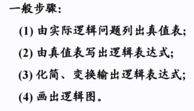
分析步骤:
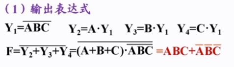
1.根据电路图,写出表达式
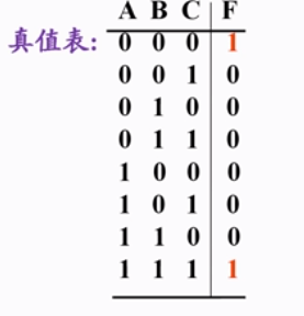
2.根据表达式,写出真值表
3.根据真值表,分析电路功能
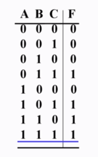
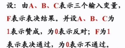
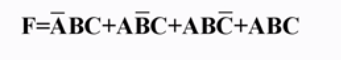
举例说明:
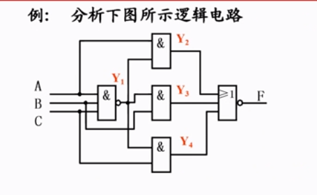
此题可按照上面的步骤一步一步解决
列出真值表
由逻辑门构成的组合电路设计方法
由逻辑门构成的组合电路设计方法

按照惯例,先列出真值表
然后写表达式
化简表达式,利用卡诺图
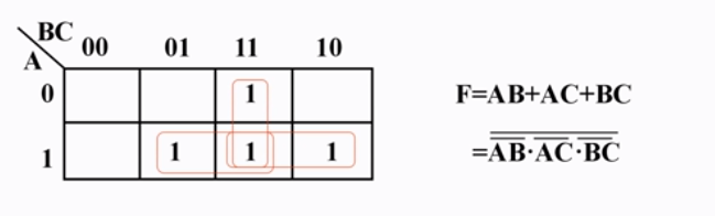
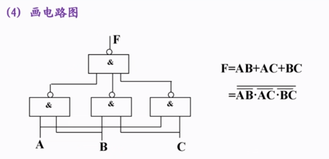
最后一步画出电路图
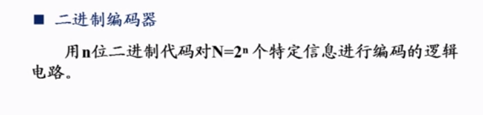
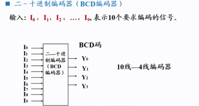
编码器
二进制编码器与BCD编码器


优先编码器只对最优先的那一个进行编码,更有价值
举个例子
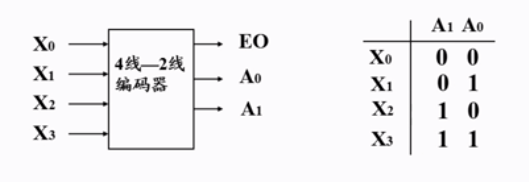
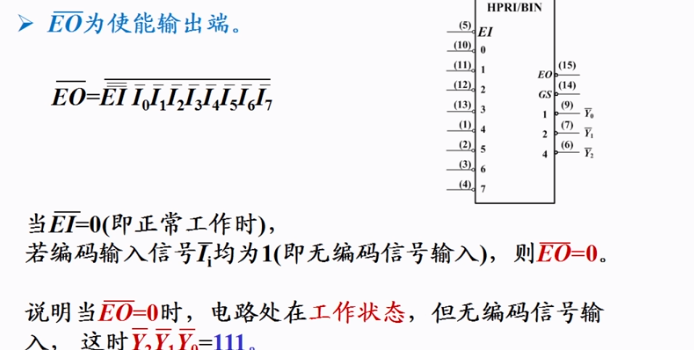
EO为使能输出
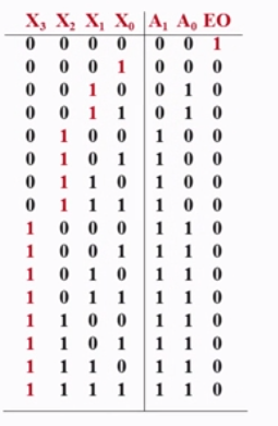
输入两个都有1时,按照优先级来
8线-3线编码器74148
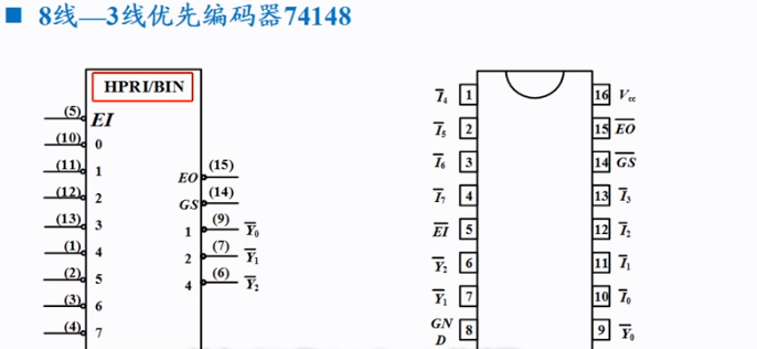
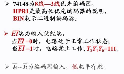
低电平有效
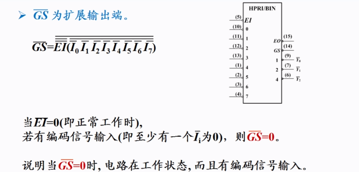
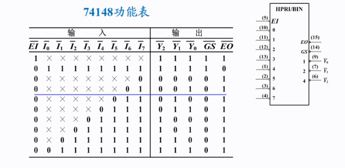
当有至少1个输入信号时,GS'=0
使能输出端,扩展输出端用来级联扩展
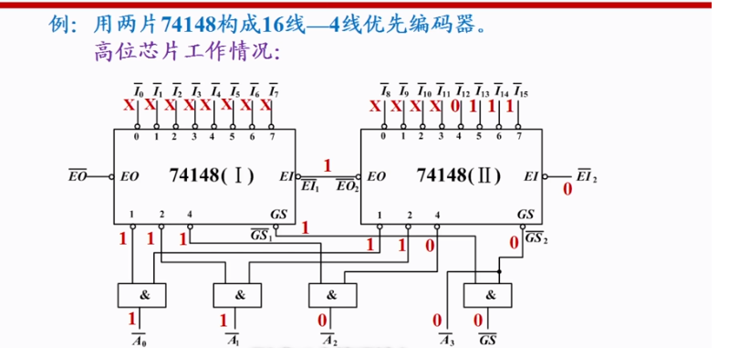
II接高八位,I接低八位
观察可得,左边EI为1,所以说左边芯片不工作,观察74148功能表可得,左边芯片输出全为1,所以A’也为1,以此类推,有兴趣的读者可以自行研究一下。
版权声明: 本文为 InfoQ 作者【顾洋琛】的原创文章。
原文链接:【http://xie.infoq.cn/article/d40e4b21455d26646b2087c1c】。文章转载请联系作者。

大二学生一名,在不断学习进步中,冲冲冲! 2020.04.30 加入
还未添加个人简介


评论